Keysight Launches Chiplet PHY Designer
New product leverages Keysight EDA’s technology and history of success simulating complex physical layer standards such as SerDes and memory.
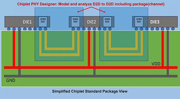
Simplified chiplet standard package view. Image courtesy of Keysight Technologies.


Latest News
January 26, 2024
Keysight Technologies, Inc. introduces Chiplet PHY Designer, the latest in its family of high-speed digital design and simulation tools that provides die-to-die (D2D) interconnect simulation, a key step in verifying performance for heterogeneous and 3D integrated circuit (IC) designs (chiplets).
The new electronic design automation (EDA) tool can provide in-depth modeling and simulation capabilities that enable chiplet designers to verify that their designs meet specifications of the Universal Chiplet Interconnect Express (UCIe) standard.
UCIe is a chiplet interconnect specification in the semiconductor industry. It is an open standard that defines the interconnect between chiplets within an advanced 2.5D or 3D package. UCIe is in process of being supported or adopted by many of the top semiconductor equipment and EDA tool vendors as well as foundries and chiplet designers. Designers who use the interconnect standard and ensure their chiplets perform to its specifications are helping establish a broad ecosystem for chiplet interoperability and commerce, according to Keysight.
Keysight EDA's research and development team has been working on modeling and simulating high-speed digital interfaces aligned with industry specifications for decades. For example, ADS Memory Designer offers memory interface coverage such as GDDR7, DDR5, LPDDR5, and HBM3 with its IBIS-AMI modeler. Its JEDEC compliance test solution handles over 100 test IDs with the same test algorithm found in the Keysight Infinium oscilloscope family.
Key features of the Chiplet PHY Designer physical-layer simulator include:
- Supports UCIe physical layer standard—automated parsing of signals following the standard naming conventions, automated connections between multiple dies through package interconnects, standard driven simulation setup such as speed grade, and intuitive measurement setup through specialized probe component.
- Analysis of forwarded clocking to accurately capture the asynchronous clocking behavior.
“Our high-speed digital simulation team capitalized on its understanding of the shift left challenges presented by SerDes PHYS,” says Niels Faché, vice president and general manager, Keysight EDA, says. “They have applied these learnings to the chiplet domain to extend success of our standards-based simulation strategy to UCIe. Interconnect modeling is critical to system design and performance.
“Chiplet PHY Designer accelerates validation of chiplet subsystems, from one D2D PHY through interconnect channels to another D2D PHY, much earlier in the design cycle,” Faché adds. “It enables 3D IC designers to solve critical interconnect performance problems improving predictive virtual prototyping to speed time-to-market.”
Sources: Press materials received from the company and additional information gleaned from the company’s website.
More Keysight Technologies Coverage
Subscribe to our FREE magazine, FREE email newsletters or both!
Latest News
About the Author
DE’s editors contribute news and new product announcements to Digital Engineering.
Press releases may be sent to them via [email protected].