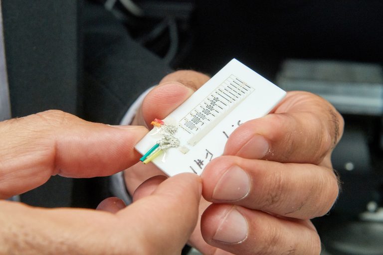
New smart sensors will include printed electronics embedded in the components. Image courtesy of University of Connecticut.
Latest News
August 27, 2018
If the future of manufacturing lies with smart or connected machines, then those machines will need a wide variety of sensors. The United Technologies Research Center and researchers at the University of Connecticut (UConn) are leveraging 3D printing technology to create wear sensors that can let operators know when a machine is damaged.
The scientists involved in the project are using direct-write technology and metallic ink to create fine lines of conductive filament that are embedded in 3D-printed machine components as they are being produced. The printed electronics create a sensor within the part that can detect wear and other types of damage.
“We can now integrate functions into components to make them more intelligent. These sensors can detect any kind of wear, even corrosion, and report that information to the end user. This helps us improve performance, avoid failures, and save costs,” said Sameh Dardona, associate director of research and innovation at UTRC.
According to a release from the University of Connecticut, this is how the sensors operate:
“Parallel lines of silver filament, each coupled with a tiny 3D-printed resistor, are embedded into a component. The interconnected lines form an electrical circuit when voltage is applied. As lines are embedded deeper and deeper into a component from the surface, each new line and resistor are assigned an increasingly higher voltage value. Any damage to the component, such as wear or abrasion caused by friction from moving parts, would cut into one or more of the lines, breaking the circuit at that stage. The more lines that are broken, the greater the damage. Real time voltage readings allow engineers to assess potential damage and wear to a component without having to take an entire machine apart.”
In practical applications, the technology could be used to monitor cracking or wear on a jet engine turbine blade, for example, by detecting blade damage that isn’t otherwise visible.
The team was able to embed sensor lines that were 15 microns wide and 50 microns apart in its tests. They were also able to create components that had magnetic coatings or magnetic materials embedded within, and produce them in a variety of shapes and sizes. They used low-temperature UV light to cure the magnets, which improved their magnetic properties compared to other processes.
You can read more about the research in Additive Manufacturing and in the Journal of Magnetism and Magnetic Materials.
Source: University of Connecticut
Subscribe to our FREE magazine, FREE email newsletters or both!
Latest News
About the Author
Brian Albright is the editorial director of Digital Engineering. Contact him at [email protected].
Follow DE


