Hardware-Software Design Optimization
New tools for electronic system prototyping are speeding design testing.
Design Exploration and Optimization News
Design Exploration and Optimization Resources


Latest News
January 1, 2013
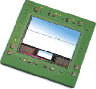 Engineers designing electronic systems likely have experience working with field-programmable gate arrays (FPGAs), programmable hardware chips that can be overlaid with logic to create electronic components—and even entire systems. These chips provide the ability to quickly configure and customize electronic devices after manufacturing, in the field.
In many cases, FPGAs and similar logic chips are also used to prototype complete electronic systems that are used in system-on-a-chip designs that deliver full processing and input-output functionality for applications like mobile phones and automotive electronics. These prototypes are then cast into application-specific integrated circuits (ASICs) for performance and manufacturability, and used in complex hardware-software systems.
But engineers can have a difficult time working with FPGAs, and deeply embedded systems in general. FPGAs and other logic devices have hundreds of thousands, or even as many as tens of millions of logic gates, and programming them using traditional hardware definition languages can be a challenge. Most designers prefer working with pre-defined logic components, referred to as intellectual property, or IP. These are hardware description language (HDL) programs that define a particular function, such as a processor, I/O interface like USB, or even graphics.
Further, these systems are almost always customized with software. An automotive braking system, for example, uses a processor, I/O for data inputs and instructions, and storage. But it is also coded with explicit instructions on how to interpret and respond to data inputs, and how to handle data and processing errors.
This embedded software is difficult to develop while the hardware design and implementation are still in flux. Interfaces, timing and even performance aren t usually fully defined until the hardware system is designed and the components selected. That puts software development behind the hardware, typically at the very end of the project. Putting software last often has undesirable consequences, such as poor performance, bad design, incomplete or missing features, and poor testing.
Building Virtual Prototypes in Logic Devices
In prototyping, electronic designers partition the FPGA logic chips and position the IP logic onto the chip, then design interfaces so that they work together in providing the needed functionality. While this may not be the final design, work on the software can begin as soon as there is an initial prototype of the hardware on the FPGA. The resulting circuit is then tested for functionality in the larger system, or within a testing harness.
Once hardware is finalized, it can be placed on the FPGA and the software can be completed. The device can be used as-is, if the end product is custom or for a small manufacturing run. For large runs, the FPGA can be produced as an ASIC or a system on a chip (SOC), and the costs spread over a larger product base.
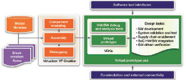 A typical design flow for embedded software optimization of electronic hardware-software systems, using TLM Central system models and the Virtual Development Kit. |
This prototyping process sounds straightforward, but it often isn t. IP blocks can be difficult to work with, especially if multiple blocks are being used on a single chip. Often, the position, layout and interfaces of these blocks can influence both the capacity and performance of the resulting circuit. Sloppy design can easily result in not meeting product specs or performance. As embedded electronic systems become more complex, the costs of bad design and placement become more significant.
Vendors such as Xilinx and Altera make the FPGAs and other programmable logic devices that are used in prototyping these embedded software systems. The hardware description languages are standard across the industry. The competitive advantage in creating prototypes comes in the placement and mapping software that determines the optimal places for IP blocks on a chip. The best approaches to prototyping can save significant time and chip expenses over manual methods.
Hardware-Software Co-development
An initiative by the programmable logic industry is making it possible to do more embedded software development as a part of the hardware prototyping process. This initiative, called TLM Central, consists of a portal, a set of high-level descriptions and models of standard hardware components in the SystemC language, and comprehensive information on how to create and manage virtual prototypes.
These virtual prototyping systems are integrated with an intelligent prototyping software environment that enables faster partitioning, and automates the creation and debugging of prototypes for a range of designs—from individual IP blocks and processor sub-systems to complete SOC, easing the path from concept to operational prototype. Engineers can use the on-chip virtual prototype as a platform for loading an operating system, coding control and management software unique to the product.
The important part of the process is that the FPGA-based prototype is used for software development while the hardware is still being defined. The TLM Central solution includes a set of freely available software development components integrated into the engineer s software development environment.
According to Tom De Schutter, senior product marketing manager, System Level Solutions at founding member Synopsys, the more engineers that use TLM Central, the more valuable it becomes: “With over 1,000 hardware component models, engineers can build virtual simulations of a wide variety of hardware-based embedded systems in many different industries.”
The accompanying software environment, called a Virtual Development Kit, incorporates popular software debuggers, system control mechanisms, and debugging information. To work with a virtual prototype, engineers install and start using—there s no need to wait for a hardware prototype to develop software.
Possibly the biggest advantage in this approach is a reduction of project risk. Any major issues with the software can be worked out more easily, either through redesigning interfaces or substituting other hardware components.
Engineers engaged in complex hardware-software system design in mobile communication, automotive, aerospace and similar industries are often faced with a rush to complete software development and integration once the hardware is in place. Using a virtual prototype of an FPGA and TLM Central-based system models, designers can begin work on the software systems before the hardware components are fully defined. Once final silicon is ready, either on an FPGA or ASIC, product designers can finalize the software much more quickly. Most important, there is no need to wait until final silicon to begin software development.
It s not a panacea, of course. Any software written before final silicon will have to be tested—and likely undergo some changes once it is able to run on actual hardware. And while the two can be developed more or less in parallel, the software will always take longer. But using a virtual prototype can reduce risk at the same time it accelerates time to market for an optimized design. DE
Contributing Editor Peter Varhol covers the HPC and IT beat for DE. His expertise is software development, math systems, and systems management. You can reach him at [email protected].
MORE INFO
Subscribe to our FREE magazine, FREE email newsletters or both!
Latest News
About the Author
Peter VarholContributing Editor Peter Varhol covers the HPC and IT beat for Digital Engineering. His expertise is software development, math systems, and systems management. You can reach him at [email protected].
Follow DE