Native 3D visualizations and clearance checking in Altium Designer enable you to see in real-time exactly how your board will fit a mechanical enclosure. Collision errors can be fixed quickly using the software’s 3D editing tools. Image courtesy of Altium Ltd.
Latest News
January 13, 2016
Altium Ltd. has announced version 16 of its flagship PCB (printed circuit board) design environment, Altium Designer. Describing this release as “a major update,” the company says version 16 expands the Altium Designer platform with several new features that enhance design productivity and automation, allowing engineers to create complex, error-free designs in less time. Among those cited by the company are Alternative Part Choice, Component Placement and Offline Design systems, as well as Visual Clearance Boundaries, a 3D STEP model generation wizard and an integrated TASKING Pin Mapper.
Altium Designer 16’s Alternative Part Choice system provides designers full control over the component selection process for manufacturing, reports the company. With it, designers can specify alternate component choices as they design. Designers can also include pin-compatible backup part selections in their BOM (bill of materials) directly and, if the need arises, automatically substitute part numbers.
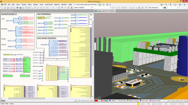 Altium has released version 16 of its flagship PCB (printed circuit board) design tool, Altium Designer. This native 3D design solution sees the introduction of several new features that enhance design productivity and automation. Image courtesy of Altium Ltd.
The Component Placement System offers Altium Designer 16 users several new component placement options for creating well-organized and efficient board layouts, according to the company. Features include the ability to dynamically place and drag components that push, avoid and snap-to alignment with other components on a board layout.
The Offline Design System provides a variety of connectivity sharing options that designers can use to fully control what network data they share with the outside world. Connectivity for applications within Altium Designer, preferences sharing, licensing servers and part supplier connections are some of the data that can be specified.
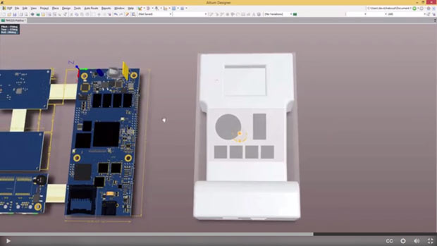
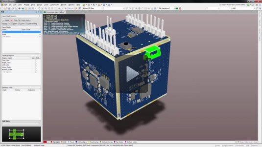 Altium Designer supports rigid-flex PCB design. This video screenshot shows how Altium Designer helps you define material selections, intelligently route your rigid-flex board layout and then visualize your work in 3D. Image courtesy of Altium Ltd.
Altium says that version 16’s Visual Clearance Boundaries functionality allows designers to understand the impact of their routing decisions in real-time by enabling them to see clearance boundaries between traces and components they route and design. The software’s 3D STEP model generation wizard allows designers to generate realistic and accurate 3D models to provide an exact representation of a board. The integrated TASKING Pin Mapper allows designers to share design data such as pin assignments, processor chip identifiers and symbol names between an Altium Designer PCB design and the TASKING toolset for embedded software projects.
 Native 3D visualizations and clearance checking in Altium Designer enable you to see in real-time exactly how your board will fit a mechanical enclosure. Collision errors can be fixed quickly using the software’s 3D editing tools. Image courtesy of Altium Ltd.
“Engineers are constantly being challenged to design PCBs in increasingly smaller product packages while still requiring the highest-performance electronics,” said Jason Hingston, CTO at Altium, in a press statement. “Altium Designer 16 empowers every engineer with the powerful capabilities needed to meet the challenges of these design demands with industry-leading productivity and automation tools found only in the unified Altium Designer platform.”
Altium Designer 16 is available now as a free upgrade to all Altium subscription customers and can be downloaded from the Altium Products Download page. For full details on Altium Designer, click here.
Click here to see what’s new in Altium Designer 16.
Access a library of Altium Designer and case studies videos.
Request a 30-day full-featured evaluation license of Altium Designer.
See why DE‘s editors selected Altium Designer 16 as their Pick of the Week.
Sources: Press materials received from the company and additional information gleaned from the company’s website.
Subscribe to our FREE magazine, FREE email newsletters or both!
Latest News
About the Author
Anthony J. Lockwood is Digital Engineering’s founding editor. He is now retired. Contact him via [email protected].
Follow DE