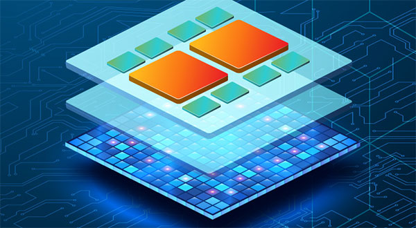
Cadence Integrity 3D-IC Platform. Image courtesy of Cadence Design Systems.
October 8, 2021
Cadence Design Systems, Inc. reports the delivery of the Cadence Integrity 3D-IC platform, a comprehensive, high-capacity 3D-IC platform that integrates 3D design planning, implementation and system analysis in a single, unified cockpit. The Integrity 3D-IC platform underpins Cadence’s third-generation 3D-IC solution, providing system-driven power, performance and area (PPA) for individual chiplets through integrated thermal, power and static timing analysis capabilities, the company reports.
Chip designers creating hyperscale computing, consumer, 5G communications, mobile and automotive applications can achieve greater productivity with the Integrity 3D-IC platform versus a disjointed die-by-die implementation approach, Cadence reports. The platform provides system planning, integrated electrothermal, static timing analysis (STA) and physical verification flows, enabling faster, high-quality 3D design closure.
It also incorporates 3D exploration flows, which take 2D design netlists to create multiple 3D stacking scenarios based on user input, automatically selecting the optimal, final 3D stacked configuration. The platform database supports all 3D design types, letting engineers create designs at multiple process nodes simultaneously and perform co-design with package design teams and outsourced semiconductor assembly and test (OSAT) companies that use Cadence Allegro packaging technologies.
For more information on the Integrity 3D-IC platform, click here.
Customers using the Integrity 3D-IC platform have access to the following features and benefits:
- Common cockpit and database: Lets SoC and package design teams co-optimize the complete system concurrently, allowing system-level feedback to be incorporated efficiently.
- Complete planning system: Incorporates a complete 3D-IC stack planning system for all types of 3D designs, enabling customers to manage and implement native 3D stacking.
- Seamless implementation tool integration: Provides ease of use through direct script-based integration with the Cadence Innovus Implementation System for high-capacity digital designs with 3D die partitioning, optimization and timing flows.
- Integrated system-level analysis capabilities: Enables robust 3D-IC design through early electrothermal and cross-die STA, which allows early system-level feedback for system-driven PPA.
- Co-design with the Virtuoso Design Environment and Allegro packaging technologies: Allows engineers to seamlessly move design data from Cadence analog and packaging environments to different parts of the system through the hierarchical database, enabling faster design closure and improved productivity.
- Easy-to-use interface: Includes a powerful user cockpit with a flow manager that provides designers with a uniform, interactive way to run relevant system-level 3D system analysis flows.
“Cadence has historically offered customers strong 3D-IC packaging solutions through its leading digital, analog and package implementation product lines,” says Dr. Chin-Chi Teng, senior vice president and general manager in the Digital & Signoff Group at Cadence. “With recent developments in advanced packaging technologies, we saw a need to further build upon our successful 3D-IC foundation, providing a more tightly integrated platform that ties our implementation technology with system-level planning and analysis. ”
The Integrity 3D-IC platform is part of the broader Cadence 3D-IC solution portfolio, which goes beyond digital and includes system and verification and IP features. The broader solution provides hardware and software co-verification and power analysis of the full system via the Dynamic Duo, which consists of the Palladium Z2 and Protium X2 platforms. It also provides connectivity via chiplet-based PHY IP with PPA optimized for latency, bandwidth and power. The Integrity 3D-IC platform offers co-design capabilities with the Virtuoso Design Environment and Allegro technologies, integrated IC signoff extraction and STA with the Quantus Extraction Solution and Tempus Timing Signoff Solution, and integrated signal integrity/power integrity (SI/PI), electromagnetic interference (EMI) and thermal analysis with the Sigrity technology portfolio, Clarity 3D Transient Solver and Celsius Thermal Solver.
Sources: Press materials received from the company and additional information gleaned from the company’s website.
More Cadence Coverage
Subscribe to our FREE magazine, FREE email newsletters or both!
About the Author
DE’s editors contribute news and new product announcements to Digital Engineering.
Press releases may be sent to them via [email protected].


