3D Printing Inches Toward Electronics
Additive manufacturing adoption in electronics has lagged behind other sectors, but advances in materials and processes are driving experimental use cases.
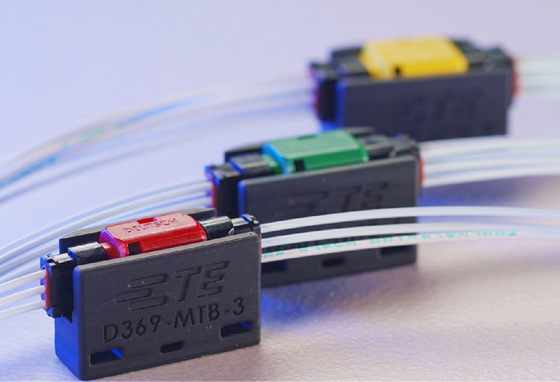
TE Connectivity taps Stratasys’ Origin One to achieve double-digit micron accuracy in mass production of aerospace connector holders. Image courtesy of Stratasys.

Latest News
September 8, 2021
3D printing has become a transformative tool for consolidating parts in automotive and aerospace applications and for producing bespoke medical equipment, yet the technology has made far less headway in electronics innovation due to an array of challenges related to materials and performance.
That dynamic is starting to shift, albeit ever so slightly. A flurry of developments on many fronts—among them, new metal, ceramic and compound materials; conductive inks for creating traces on circuits; thin-film delaminated electronics; and high-precision, specialized hardware and processes—are empowering emerging additive manufacturing (AM) platforms to tackle the unique challenges related to electronics component and device production.
Advances in metal 3D printing technology are making it easier and more cost effective to produce the complex manifolds, wafer tables and wafer handling systems found in semiconductor lithography and wafer processing equipment.
Although most use cases are still relatively early stage—typically exploratory research and development efforts or pilot applications—there are various advantages that 3D printing technologies bring to electronics production. The primary benefits, according to experts, are simplification, accelerated time to market, ease of customization and greater design freedom. In the right scenario and for a specific type of parts, there is potential for cost reduction through elimination of expensive injection molds and tooling.
“If you can break the trade-off between price and volume with digital manufacturing, you can make the jump towards mass customization,” says Matthew Dyson, senior technical analyst at market research firm IDTechX. “At present, additive manufacturing [of electronics] is not best suited for making large volumes. But for low volumes with lots of variation or some bespoke aspect, then there can be a lot of benefits to an AM approach.”
What’s Holding Things Back?
The lack of material choice and the limited capabilities of currently available materials are among the primary inhibitors restricting widespread use of 3D printing for electronics applications.
Transducers, sensors, antennas and batteries call for highly sophisticated properties, which are difficult to replicate with the current portfolio of materials associated with most existing 3D printing platforms.
“It’s much easier to define the requirements for traditional 3D-printed structural materials in terms of yield stress or whether it will meet the required performance for the application,” says Karl Littau, chief technology officer at Sakuu, a company working on a specialized 3D printer for producing electric vehicle (EV) batteries.
With functional devices such as batteries, multiple materials are involved, and each have specific density and structural requirements that must be met simultaneously.
“At a minimum in an electronics device, you have an insulator and a conductor and with that requirement alone, you’ve eliminated 99% of current 3D printers,” Littau says. “It’s not a common ability of AM to deposit the conductor and dielectric in the same machine in the same part, side by side. For those reasons, the AM world has focused on the more traditional elements of 3D printing.”
In comparison, Sakuu offers a multiple-AM platform that blends powder bed and jetted material deposition processes and can employ different multimaterials in a single layer capability. The process combines ceramic and metal, along with Sakuu’s proprietary support material, that results in an ability to quickly create high-energy density solid-state batteries (SSBs) with thin monolithic layers using an approach that encourages easier recyclability of materials compared to conventional methods, Littau says.
Sakuu is targeting players in the e-mobility space initially, but anticipates the 3D printer having applicability for a range of applications in different sectors. Sakuu also markets its own KeraCel brand of SSBs produced with the Sakuu AM Platform.
Because structural elements are commonly made out of plastic and electronics components drawn from metal materials, different thermal and mechanical properties are required; combining the two in a singular 3D printing process introduces further complexity not yet addressed by most current systems, says IDTechX’s Dyson.
“Managing the close proximity of materials with different properties and how to respond to temperature cycling is a significant challenge,” he says. The ability to achieve high yields before fully committing to 3D printing is another barrier that needs to be overcome before moving from prototyping to full production.
“If a problem like a dodgy connection is buried inside a part, you have to throw the whole part away,” he adds. “There is no way a person or robot can make that repair.”
Performance characteristics and surface finish capabilities are another barrier limiting more widespread use of 3D printing in the electronics arena. Traditional Fused Deposition Modeling (FDM) printers can’t produce the quality and surface finishes required for some consumer electronics applications while stereolithography (SLA) offerings can accommodate the intricate features so critical to components in this space, yet there isn’t the same deep bench of materials advancements, says Chris Prucha, vice president of Origin P3 at Stratasys, and co-founder of Origin.
“Even the materials used five years ago didn’t have the toughness and properties we needed out of a commercial-grade material for something like electrical connectors,” says Prucha, who underscores the need for characteristics such as flame retardancy or the toughness and surface finishes associated with composites.
“Our technology marries the high quality and expanding materials portfolio of FDM with a high quality and high throughput print process.”
Innovations on the Horizon
TE Connectivity, which produces upwards of 190 billion sensors and connector products annually, has been eying 3D printing as a more time-efficient and cost-effective way to produce portions of its product line, especially for those electrical connectors made in low volumes for aerospace applications. Rather than having to spend the time and money to build expensive tooling for parts made in the tens or maybe hundreds of thousands, TE saw promise in 3D printing as a way to get to the best possible design solution much more quickly.
Yet finding a solution that could meet TE’s requirement for high-precision accuracy was a problem. “3D printing technologies were either high resolution with low material properties or offered good material properties, but had laminated or crude surface faces,” says Mark Savage, research and development senior manager, additive manufacturing at TE.
Stratasys’ Origin printer, with its digital light processing (DLP) technology and expanded palette of materials, provided a way to achieve components with robust material properties and high surface resolution and accuracy.
Consider one aerospace application where a single connector could have as many as 60 pins that slot into corresponding holes, which demand tolerances in the single micron range, Savage says. “We’re always pushing the limits of what 3D printing can give us, whether that’s tight tolerances or exotic materials,” he adds.
One area where 3D printing already has a notable impact in the electronics sector is increased performance and productivity of semiconductor capital equipment. Metal AM technologies, when applied to semiconductor lithography and wafer processing equipment, can be used for liquid cooling applications, including for the design of complex metal AM parts such as manifolds and wafer tables that help optimize fluid and gas flow to reduce pressure drops and minimize mechanical disturbances and vibration.
Unlike traditional manufacturing methods, metal AM can create and output manifolds that consolidate parts, are lighter in weight and volume, and can optimize fluid flow, says Scott Green, principal solutions leader for 3D Systems.
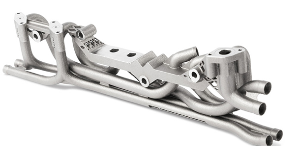
AM-built manifolds optimize performance for semiconductor equipment characterized by densely packed components containing many fluid channels in a clean environment. Image courtesy of 3D Systems.
Another potential upside of 3D printing for electronics components and devices is the possibility of increased design freedom. Similar to how the combination of 3D printing and generative design software unleashed a new generation of lightweight, organic-shaped components that weren’t possible to produce with traditional manufacturing methods, new 3D printing technologies would make it possible to rethink traditional designs via an ability to integrate the electronics directly within or onto product surfaces in an approach IDTechX’s Dyson calls “fully additive.”
This longer-term vision applies 3D printing to the structural and electronic aspects of a device, ensuring there are no constraints on how conductive traces are distributed within a structural dielectric.
Dyson believes fully additive methods, still in the early experimental stages, could find a home for producing helical antennas and integrated capacitors as well for other bespoke parts or applications where size and weight are extremely important, such as custom implants.
“By enabling electronics to be integrated into things, designers are not forced to design products that can accommodate this rectangular [printed circuit board], but rather can make any shape they like,” Dyson says, using the standard rectangular smartphone as an example.
“With an AM approach, you wouldn’t have to have a circuit board that was planar—you could make something in[to] any shape,” he says.

nScrypt 3D printed a curved phased array antenna for the U.S. Air Force. Image courtesy of nScrypt.
In the near term, the ability to 3D print electronics functionality onto existing injection molded components is already delivering advantages for experimental military and space station applications. The Sciperio research arm of nScrypt Inc., which makes high-precision industrial microdispensing and direct digital manufacturing equipment, is working with the U.S. Air Force Research Laboratory to print a phased antenna array on a curved surface.
This feat is possible due to the company’s platform, which combines high-precision motion control, surface mapping, multi-camera machine vision, aerosol jetting as well as other milling and polishing processes into a single platform, according to Kenneth Church, nScrypt CEO.
“You can print, mill, polish and postprocess in one system and do it spot by spot, layer by layer so you can build the entire part on the system,” says Church, who also touts the company’s wide range of materials—over 10,000 can run in the system.
More 3D Systems Coverage
More Stratasys Coverage
Subscribe to our FREE magazine, FREE email newsletters or both!
Latest News
About the Author
Beth Stackpole is a contributing editor to Digital Engineering. Send e-mail about this article to [email protected].
Follow DE

